 Fundraising Fox
大熊ダイヤモンドデバイス株式会社
Sapporo, JP · 14 known investors
Find your way into 大熊ダイヤモンドデバイス株式会社
Ookuma Diamond Device develops diamond semiconductor technology, aiming to apply diamond-based devices across various fields. The company is based in Japan.
Also known as Ookuma Diamond Device · OOKUMA DIAMOND DEVICE Co., Ltd. · 大熊ダイヤモンドデバイス
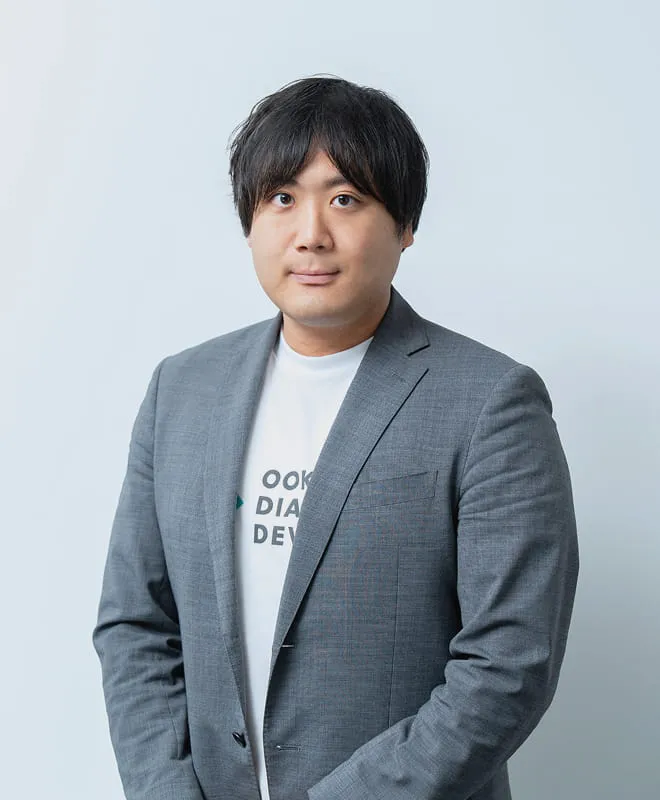
Founders & leadership
Investors · 14
How we know: the company's own site · research · initial.inc · Not right? Tell us

How we know: Coral Capital's portfolio page · the company's own site · the VCSheet dataset · research · initial.inc · Not right? Tell us
How we know: Globis Capital Partners's portfolio page · the company's own site · research · initial.inc · Not right? Tell us
How we know: the company's own site · research · initial.inc · Not right? Tell us
How we know: the company's own site · research · initial.inc · Not right? Tell us
How we know: the company's own site · research · initial.inc · Not right? Tell us
How we know: the company's own site · research · initial.inc · Not right? Tell us
.png)
How we know: the VCSheet dataset · research · initial.inc · Not right? Tell us
Also in the syndicate · 6
Company profile
researched Aug 2026大熊ダイヤモンドデバイス株式会社 (Ookuma Diamond Device Co., Ltd.) is a Japanese semiconductor company founded in March 2022, headquartered in the Hokudai Business Spring facility in Kita-ku, Sapporo, Hokkaido. It originates from research at Hokkaido University and the National Institute of Advanced Industrial Science and Technology (AIST), and describes itself as a university- and public-research-institute-derived startup. Its stated mission is to create a Japan-originated next-generation semiconductor industry through contributing to the decommissioning of the Fukushima Daiichi Nuclear Power Station.
The company researches, develops, manufactures and sells diamond semiconductor materials, substrates and devices. Diamond semiconductors are positioned as a successor to silicon, SiC and GaN, offering high-frequency performance, high power efficiency and heat dissipation, and the ability to operate in high-radiation and high- or low-temperature environments without requiring heat removal, in compact and lightweight form. Product and application areas include radiation measurement and neutron detection for nuclear power plants and severe-accident response, diamond detectors for worker safety management and acquisition of information on fuel debris inside reactors, semiconductor elements and amplifiers for satellite communications and radar, and base-station devices for Beyond 5G/6G networks.
Ookuma Diamond Device built the Ookuma Diamond Device Fukushima Plant in Okuma, Futaba District, Fukushima Prefecture, adjacent to the Fukushima Daiichi site. The two-storey steel-frame facility sits on roughly 5,800 m² with about 1,100 m² of building area within the Okuma Central Industrial Base, and was completed on 2026-05-29 as a production site dedicated to diamond semiconductor R&D and manufacturing.
Founding story
The company was established in the wake of the Great East Japan Earthquake and the Fukushima Daiichi nuclear accident, bringing together domestic research expertise developed over more than ten years of work on decommissioning challenges. It was founded on 1 March 2022 as a startup based on research at Hokkaido University and AIST, led by representative director Naohisa Hoshikawa.
Business model
The company develops and manufactures diamond semiconductor materials, substrates and devices for sale to business customers, with a dedicated production line at its Fukushima plant aimed at volume manufacturing. It is characterised as a B2B, R&D-intensive manufacturer.
Manufacture and sale of diamond semiconductors and related devices, including detectors for nuclear and decommissioning applications and semiconductor elements and amplifiers for satellite communications, radar and Beyond 5G base stations; activity is also supported by government subsidies and public research programmes.
Traction
Selected for METI's Independence/Return Support Employment Creation Company Location Subsidy (9th call, 12 of 27 applications accepted) in 2024; cumulative funding of about JPY 6.7 billion including grants within two and a half years of founding; selection for JAXA's Space Strategy Fund SX core-domain research "SX-ARK" (heat and devices) in April 2026; groundbreaking ceremony in April 2025 and plant completion in May 2026, with a dedication ceremony attended by around 200 people from ministries, local government, research institutions and financial institutions. Reported employee count of 23.
Latest developments
The Fukushima plant was completed with a ceremony on 2026-05-29 and announced on 2026-06-04; press coverage reported plans for volume production in fiscal 2028 and the establishment of a joint venture/consortium for social implementation. The CEO appeared on NIKKEI NEWS NEXT in June 2026 and on World Business Satellite in August 2026, and a Reuters Plus article about the company was published in March 2026.
▸Full profile — market position, technology, go-to-market, geography, history, risks & controversies
Market position
Positions itself as the first company to build a plant dedicated to diamond semiconductor R&D and manufacturing, based on its own survey of public information as of June 2026. Investors and the company cite Japan's lead in synthetic diamond semiconductor research, dating to gas-phase artificial diamond synthesis in the 1980s, and describe the company as being closest globally to practical commercialisation.
The company states it holds product-commercialisation know-how accumulated over more than ten years of R&D triggered by the Fukushima Daiichi accident, and that it is the only company with such know-how; it was also the first to begin construction of a diamond semiconductor factory.
Technology
Diamond semiconductor technology, referred to as the "ultimate semiconductor," built on more than a decade of research and development linked to Hokkaido University and AIST. The material offers superior high-frequency characteristics, high-power efficiency and heat dissipation relative to existing semiconductors, and operates under high radiation and extreme temperatures, allowing compact, lightweight devices that do not require heat removal. Applications developed include radiation measurement, neutron detection, severe-accident-response instrumentation, and high-output amplifiers.
Go-to-market
Works with government ministries and public bodies including the Cabinet Office, METI, the Ministry of Internal Affairs and Communications, the Reconstruction Agency, the Acquisition, Technology & Logistics Agency, Fukushima Prefecture, JAEA and private companies on joint projects, and pursues national programmes and subsidies alongside commercial device sales.
Nuclear decommissioning and nuclear power plant operators, space and satellite communications operators, radar and security/defence users, and next-generation (Beyond 5G/6G) communications infrastructure operators.
Geography
Headquarters in Sapporo, Hokkaido (Hokudai Business Spring, Kita 21-jo Nishi 12-2, Kita-ku); manufacturing plant in Okuma, Futaba District, Fukushima Prefecture, within the Okuma Central Industrial Base.
History
Founded in March 2022 in Sapporo. Raised a seed round of about JPY 140 million in May 2023, with Globis Capital Partners making its first investment that month. In October 2024 it announced a Pre-Series A round of approximately JPY 4 billion including debt, alongside selection for a METI plant-location subsidy, to build a diamond semiconductor factory in Okuma, Fukushima. A groundbreaking ceremony was held in April 2025, and the Fukushima plant was completed on 29 May 2026, with full-scale operation and volume production reported for fiscal 2028. In April 2026 the company was selected for JAXA's Space Strategy Fund SX-ARK research programme.
Risks & controversies
As a research-and-development-intensive deep-tech company, investors note that executing to plan is difficult in this category; the business depends on commercialising a technology previously described as twenty years away, on volume production starting from the new Fukushima plant, and on public programmes and subsidies tied to Fukushima reconstruction policy.
Compiled by commissioned research from 8 cited public sources — announcements, filings, and press listed under research sources below.
Key figures
latest reportedCompany-reported or press-reported figures, each dated to when it was claimed — not independently audited.
Timeline · 6
launches, deals, and filingsThe Fukushima plant in Okuma, Futaba District, Fukushima Prefecture was completed and a dedication ceremony held on 2026-05-29, attended by roughly 200 representatives of ministries, local government, research institutions, partner companies and financial institutions. The two-storey steel-frame facility occupies about 5,800 sqm of land with about 1,100 sqm of building area and hosts a dedicated line for diamond semiconductor R&D and manufacturing, including detectors for decommissioning and elements and amplifiers for space, security and next-generation communications.
Selected for the SX core-domain advanced research "SX-ARK" (heat and devices) under JAXA's Space Strategy Fund programme.
The company held a groundbreaking ceremony for what it describes as the world's first diamond semiconductor factory.
Pre-A round led by existing investor Globis Capital Partners, with Mizuho Bank as lead financial institution for the debt financing. Proceeds are directed at building a diamond semiconductor factory in Okuma, Fukushima. Cumulative funding since founding reached about JPY 6.7 billion including grants.
Selected in the 9th call of METI's Independence/Return Support Employment Creation Company Location Subsidy (manufacturing and service business location support), which provides up to JPY 3 billion for new or expanded plants; 12 of 27 applications were accepted.
The company raised about JPY 140 million in a seed round; Globis Capital Partners made its first investment in May 2023 and Coral Capital also participated at the seed stage.
Dated company events from announcements, filings, and press; legal rows summarize public dockets and regulator releases.
▸Research sources · 8
primary sources listed
- 大熊ダイヤモンドデバイス株式会社ookuma-dd.com · web
8 public sources were cited for this profile; the first-party ones are listed here.
Frequently asked questions
- What does 大熊ダイヤモンドデバイス株式会社 do?
- Japanese deep-tech startup developing and manufacturing diamond semiconductors for decommissioning, space, defense and next-generation communications.
- Who are 大熊ダイヤモンドデバイス株式会社's investors?
- 大熊ダイヤモンドデバイス株式会社's investors include aSTART, Coral Capital, Globis Capital Partners, FFG Venture Business Partners, Hokuhoku Capital, Mitsui Sumitomo Insurance Capital, SMBC Venture Capital, Aozora Corporate Investment.
- Where is 大熊ダイヤモンドデバイス株式会社 headquartered?
- 大熊ダイヤモンドデバイス株式会社 is headquartered in Sapporo, JP.